
The second project for the BeMicro CV board will be a HW/SW LED flasher. From the LEDs present in the board, some will be flashed by HW, and others will be flashed by SW running on a NIOS processor.
For an introduction about the Be Micro CV evaluation board, please refer to this post.
What will the project do:
- Flash a sequence of HW LEDs by dividing the clock input
- Make a ‘lamp test’ (all LEDs lit) when reset is pressed
- LEDs sequence is accelerated if the user presses the second push button on the board.
- Three LEDs are flashed by SW. To differentiate between the two groups, the LEDs flashed by SW run faster.
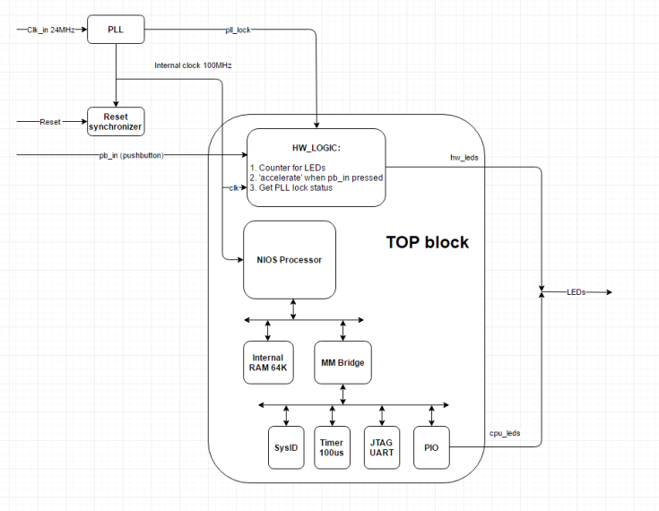
The design includes the following blocks:
- PLL: Takes the 24MHz input to the board and generates an internal 100MHz clock signal.
- Reset synchronizer: Reset signal is sampled by this block using two flip-flops. Reset is released only on rising edge of internal 100MHz clock. This is the recommended reset connection by Altera for avoiding recovery and removal timing failures. Actually the result is to connect a synchronized reset to the async. reset input of all FFs in the design.
- top block: Includes a counter to divide the input frequency to blink the LEDs at a speed visible to humans. Also takes care of reset treatment (all LEDs lit) and of LEDs blink acceleration.
- NIOS processor, together with its blocks (memory, UART, etc.), running SW that blinks three additional LEDs. The SW has a simple delay loop to increment a counter. The value of the counter is written to the GPIO register who lits the SW LEDs.
In the video, the LED at the left is the PLL lock LED. Then there are four LEDs flashed by HW (slower) and finally three LEDs flashed by SW (faster).
The design also includes the following files:
- QSF including pin assignment
- SDC – Timing constraint file
- vhdl source files
- qip files for Altera generated IP sources
- nios.sopcinfo – Used to generate the system.h to run Nios SW
Design directories structure:
- qsys: includes the NIOS HW description and its peripherals and the NIOS.vhd file
- quartus: project files, .qsf file, .sdc file
- software
- led_flasher with C source files
- led_flasher_BSP, Board Support Package directory
- src
- top.vhd and reset_sync.vhd source files
- ip directory
- pll1 directory
- files generated by Altera IP Wizard for ‘pll1’ (24MHz -> 100 MHz)
- pll1 directory
- workspace: Used by Eclipse Software IDE
The design was generated using Quartus Prime 15.1 and Eclipse Tools for Nios. The complete project directory is available here.
If you are completely new to FPGA and you want step by step instructions to generate an FPGA and/or a SW project for the Nios processor, please refer to the following links:
